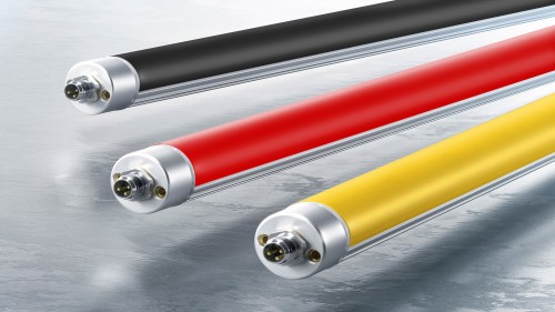
In semiconductor production, precise lighting is not just about visibility – it's mission-critical. During photolithography, photosensitive resists (photoresists) are applied to wafers that can unintentionally cure or lose their structurability with even the slightest UV exposure. Conventional lighting contains UV components that jeopardize these processes.
Yellow light for semiconductor manufacturing solves this problem through targeted spectral filtering. Photolithography lighting operates in a tightly defined wavelength range around 590 nm – the so-called amber spectrum. This range provides sufficient brightness for precise workflows while containing no critical UV components below 500 nm that could damage photosensitive materials.
Especially in ISO Class 5 to 7 cleanrooms, where wafers are processed, transported, or inspected, UV-safe lighting is essential. DIANA cleanroom yellow light meets these requirements through precise spectral control, homogeneous illumination, and full cleanroom compatibility. Benefit from decades of experience from real semiconductor and cleanroom projects: Our practical knowledge from hundreds of realized applications flows directly into the development of every luminaire – whether standard solution or custom integration.